
Lip-Bu Tan Overhauls Intel Chip Design with 'A0' Perfection Mandate
The chip design world just got a massive shakeup. What happens when a tech giant realizes its core process is suffering from quality fatigue? The answer, according to Intel CEO Lip-Bu Tan, is a radical overhaul of internal culture, demanding a level of perfection previously considered aspirational.
This isn't just another memo. This is a fundamental shift in how Intel views quality control, directly impacting every chip that leaves the facility. The new focus on rigorous standards means that the entire process of chip development is being rewritten from the ground up, signaling a major pivot in the company's commitment to performance and reliability.
What this means for players: The long-term goal is undeniable stability and performance, meaning future Intel hardware should theoretically hit higher benchmarks for reliability and efficiency.
The magnitude of the changes suggests that the era of lax quality assurance is over. The push for excellence represents a massive corporate effort to redefine the standard for the entire semiconductor industry, specifically around the **Intel CEO chip design culture changes**.
Setting the New Standard: The ‘A0’ Milestone

At the heart of this mandate is a single, critical milestone: 'A0.' For those unfamiliar with the semiconductor process, A0 represents the final, most critical pass—the moment of "tape-out." It is the point of no return, where the design is committed to physical manufacturing.
Previously, the process was viewed as a series of gates, but Lip-Bu Tan has explicitly defined A0 as the definitive line in the sand. Achieving A0 perfection is no longer optional; it is the absolute minimum requirement for moving forward.
This mandate establishes A0 as the gold standard for quality assurance. It means that every single aspect of the chip design—from the smallest transistor to the largest IP block—must be flawless before it can be certified for production. This raises the stakes significantly for every engineer involved in the design process.
Zero Tolerance for Design Flaws

The tone set by the CEO is uncompromising. He has not only mandated a new culture but has backed it with severe accountability measures. Failure to meet the new, stringent benchmarks is not merely a performance warning; it is treated as a critical failure of process.
Tan signaled that the previous culture lacked the necessary rigor, leading to unacceptable risks. The message is clear: operating at anything less than perfect—specifically, falling back to a 'B0' status—could result in immediate and serious professional consequences. This is a powerful signal of the magnitude of the **Intel CEO chip design culture changes**.
This zero-tolerance policy is designed to instill an immediate, deep-seated sense of ownership and quality responsibility across the entire engineering department. It turns a cultural recommendation into a mandatory operational mandate, ensuring that quality is built into the process, not merely checked at the end.
Focus on Pre-Tape-Out Certification
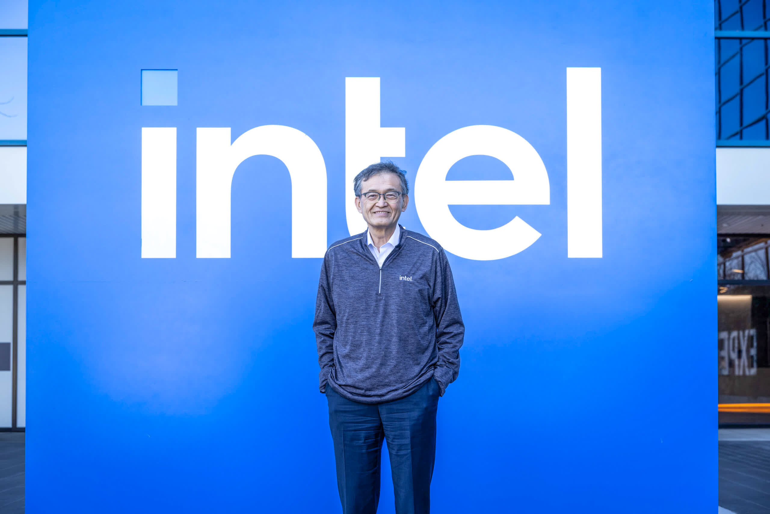
To enforce this new rigor, the focus has dramatically shifted upstream—to the pre-tape-out phase. The bulk of the effort now centers on comprehensive, deep-dive checks of every design element.
The goal is to achieve **Intel chip design bug-free production** by eliminating potential flaws *before* the design is finalized. This requires meticulous verification of all Intellectual Property (IP) cores and complex subsystem interactions. Nothing can be assumed, and nothing can be rushed.
This intensive focus on preemptive quality control ensures that the final **A0 revision tape out process** is based on the most vetted, robust data available. It represents a massive investment in process validation, designed to minimize costly and time-consuming silicon respins later down the line. This meticulous approach is key to the overall success of the new operational model.
Frequently Asked Questions
What does 'A0' mean in chip manufacturing?
A0 is the critical milestone in the chip design process, representing the final "tape-out." It signifies that the design has passed all necessary quality checks and is ready to be physically manufactured onto silicon wafers.
How will this impact future Intel product release dates?
While the immediate effect may introduce temporary delays due to the rigorous testing, the long-term goal is increased reliability. This should lead to more stable, predictable, and higher-performing products.
Is this a change to the physical chip architecture?
No, this is primarily a change in internal corporate culture and process management. It mandates a stricter, more rigorous approach to the design and verification phase, rather than changing the core architecture itself.
Industry analysts suggest that this dramatic shift in quality culture will set a new benchmark for the entire semiconductor sector. Competitors will be forced to reassess their own internal quality gates to match Intel’s new standard of operational excellence. The next few quarters will be critical in determining if this mandate can translate into verifiable, real-world performance gains.
Confirmed details first, useful context second. This is the quickest path to the source trail and the next pages worth opening.
Source date: May 20, 2026